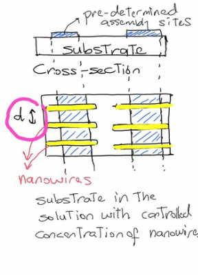
 Today, I attended a seminar at École polytechnique de Montréal, by Theresa Mayer from Pennstate University.Topic is interesting due to the reported %90 yield of the manufacturing process and its applicability to electronic applications ( sensors, transistors, ...). Usually, research is stuck in the research laboratories due to the low yield, non-scalability ( lab-scale production or % error or high expense) or because they can not find applications in the market due the limitations such as service conditions, high price of the final product etc. I digged a bit the topic and here is a quick overview of the deterministic assembly process: (Not to be mixed with self assembly of materials (SAM)) (i.e. Ghadiri, M. R., Granja, J. R., Milligan, R. A., McRee, D. E. & Khazanovich, N. Self-assembling organic nanotubes based on a cyclic peptide architecture. Nature 366, 324–327 (1993)). Deterministic assembly of nano-structures is a promising production method because it is easy and accurate. Assembly methods are named after or according to the registry driving force employed for the process. Processes using electric or magnetic fields are classified as field-directed assembly and when the capillary forces is the main influencer that is called a directed capillary assembly. The process takes place by the application of an external electric field to the nano-structures ( preferentially in a non-polar liquid at low frequency and using AC-current) which drives the nanostructures to the predetermined assembly sites. For more information you can refer to the references listed below. Company of interest: IBM Research – Zurich, Säumerstrasse 4, 8803 Rüschlikon, Switzerland
0 Comments
|
Archives
November 2017
Categories
All
|
 RSS Feed

